High-Current PCB Busbars: Materials, Design, Manufacturing & Selection Guide
High-Current PCB Busbars: Materials, Design, Manufacturing & Selection Guide
As electronic and electrical systems continue to operate at higher current levels and higher power densities, managing current capacity and heat generation has become an important part of system design.
Traditional PCB copper traces may not provide sufficient current-carrying capacity for certain high-current applications. In these situations, metal busbars, copper jumpers, and other high-current PCB connection components can provide a lower-resistance electrical path while supporting mechanical connection and thermal management.
This guide explains the materials, key characteristics, manufacturing processes, applications, and design considerations for high-current PCB busbars and metal jumper components.
What Is a PCB Busbar?
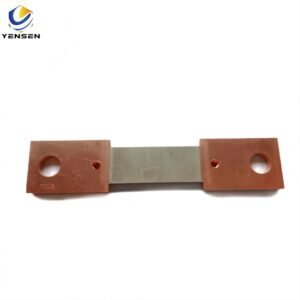
A busbar is a conductive metal component used to distribute or transfer electrical current between two or more electrical points. Unlike conventional wire connections, a busbar is typically manufactured as a flat, formed, or stamped metal component.
Common materials include copper, aluminum, brass, and specialized copper alloys.
Depending on the application and industry terminology, these components may also be described as:
- PCB busbars
- Copper busbars
- High-current PCB jumpers
- Metal bridge jumpers
- SMT busbars
- Copper jumper bars
- Current-carrying metal jumpers
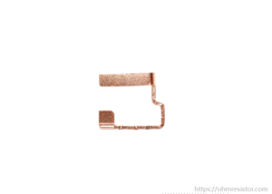
For PCB applications, a compact metal jumper can act as a low-resistance electrical bridge between circuit nodes where conventional PCB traces may not provide sufficient current capacity.
Why Use a High-Current PCB Busbar?
1. Increase Current-Carrying Capacity
A metal busbar provides a conductive path with a larger effective cross-sectional area than a conventional PCB trace.
This can be useful when high current must pass through a limited PCB area or when the required copper thickness would make the PCB more expensive or difficult to manufacture.
Depending on the design, a metal jumper can bridge two PCB points while carrying substantially higher current than a narrow copper trace.
2. Reduce Electrical Losses
The resistance of a conductor depends on its material, length, and cross-sectional area.
For a given geometry, a lower-resistivity material can reduce voltage drop and resistive power loss.
Copper is commonly selected for high-current applications because of its high electrical conductivity.
3. Support Thermal Management
Electrical resistance generates heat when current flows through a conductor.
Reducing conductor resistance can help reduce resistive losses, while the physical metal structure can also provide additional thermal conduction compared with a very small PCB trace.
However, the actual temperature rise depends on the complete thermal system, including current, conductor geometry, PCB construction, mounting conditions, airflow, and surrounding components.
4. Provide a Reliable Electrical Bridge
A stamped or formed metal jumper can provide a defined mechanical connection between PCB locations.
Compared with flexible wires, a rigid metal jumper can offer a controlled geometry and repeatable mounting position, which can be useful for automated PCB assembly.
Material Selection for PCB Busbars
Material selection depends on the required electrical conductivity, mechanical strength, thermal performance, weight, cost, and manufacturing process.
Copper
Copper is one of the most common materials for high-current conductive components because of its high electrical and thermal conductivity.
Typical advantages:
- High electrical conductivity
- Good thermal conductivity
- Suitable for stamping and forming
- Good solderability with appropriate surface treatment
- Suitable for high-current PCB applications
T2 copper is commonly used where electrical conductivity is a primary requirement.
Brass
Brass generally provides higher mechanical strength than pure copper but has lower electrical conductivity.
It can therefore be considered when mechanical rigidity or forming characteristics are more important than achieving the lowest possible electrical resistance.
Aluminum
Aluminum has lower density than copper and can reduce component weight.
It can be useful where weight is an important design consideration, although electrical conductivity, joining method, surface treatment, and manufacturing requirements must be evaluated for each application.
Material Comparison
| Material | Electrical Conductivity | Thermal Conductivity | Mechanical Strength | Typical Application |
|---|---|---|---|---|
| T2 Copper | High | High | Moderate | High-current PCB connections |
| Brass | Lower than copper | Moderate | High | Applications requiring mechanical strength |
| Aluminum | Moderate | High | Lower than brass | Weight-sensitive applications |
Actual material properties vary by alloy, temper, thickness, and applicable material standard. Final material selection should therefore be based on the specific design and operating conditions.
Surface Treatment for Copper Busbars
Copper provides excellent conductivity, but its surface can oxidize over time. Surface treatment may therefore be required depending on the connection method and environmental conditions.
Common surface treatments include:
Tin Plating
Tin plating can improve solderability and provide a suitable surface for SMT assembly.
It is commonly considered for PCB-mounted metal jumpers where soldering reliability is important.
Nickel Plating
Nickel provides a harder surface and can improve resistance to wear, oxidation, and environmental exposure.
It may be considered when improved surface durability is required.
Other Surface Treatments
The appropriate surface treatment depends on:
- Soldering method
- Operating environment
- Contact requirements
- Storage conditions
- Corrosion resistance
- Required service life
Surface treatment should be specified together with the base material and application requirements rather than selected independently.
Manufacturing Process for High-Current PCB Metal Jumpers
High-current PCB busbars and metal jumper components are commonly produced using stamping, forming, bending, surface treatment, inspection, and automated packaging processes.
1. Metal Stamping
Copper or other conductive sheet material is stamped to the required outline.
The stamping process can provide repeatable dimensions and is suitable for medium- and high-volume production.
2. Forming and Bending
After stamping, the component may be formed into the required geometry.
Depending on the design, this can include:
- U-shaped structures
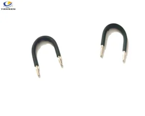
- Offset structures
- Raised bridges
- Step configurations
- Terminal bends
The final geometry should maintain sufficient clearance from surrounding components and provide reliable PCB mounting.
3. Deburring and Cleaning
After stamping and forming, burrs and metal particles should be controlled.
Suitable cleaning and finishing processes can help remove contamination and reduce the risk of assembly defects.
For soldered PCB components, controlling burrs and sharp edges is particularly important.
4. Flatness and Dimensional Inspection
Flatness and dimensional accuracy can affect PCB mounting and soldering quality.
Inspection may include:
- Overall dimensions
- Thickness
- Hole diameter
- Bend position
- Flatness
- Surface condition
- Burr inspection
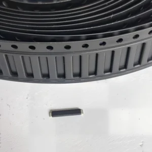
5. Tape-and-Reel Packaging
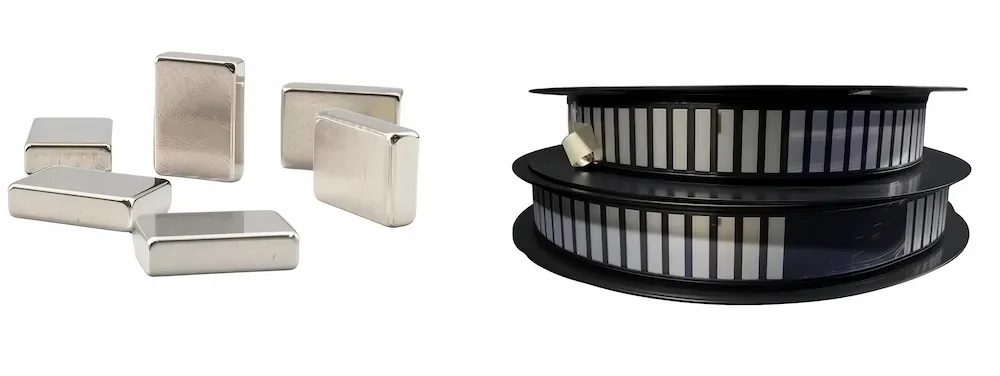
For SMT-compatible components, tape-and-reel packaging can support automated pick-and-place assembly.
Packaging design should consider component geometry, orientation, feeding stability, moisture protection, and mechanical protection during transportation.
Typical Applications
High-current PCB busbars and metal jumper components can be used in a wide range of power electronics and industrial applications.
Power Electronics
Typical applications include:
- Power converters
- DC power supplies
- Inverters
- UPS systems
- Motor control equipment
- Industrial control systems
Battery and Energy Storage Systems
Metal current-carrying components can also be used in:
- Battery management systems
- Energy storage systems
- Battery monitoring equipment
- Power distribution modules
- Charging systems
EV and Charging Equipment
High-current conductive components may be used inside:
- EV charging modules
- DC charging equipment
- Power conversion modules
- Battery power systems
The final current rating and thermal performance must always be validated against the complete system design.
PCB Busbar Design Considerations
Selecting a high-current metal jumper or PCB busbar is not simply a matter of choosing a material.
The complete electrical, mechanical, and thermal design should be considered.
1. Current Rating
The required conductor size should be determined based on:
- Continuous current
- Peak current
- Pulse duration
- Duty cycle
- Ambient temperature
- Permitted temperature rise
A component’s current rating should not be considered independently from the actual mounting and cooling conditions.
2. Cross-Sectional Area
Increasing conductor width or thickness generally reduces resistance and can increase current-carrying capability.
However, a larger cross-section also affects:
- PCB space
- component height
- solder joint design
- forming requirements
- manufacturing cost
3. Geometry and Current Distribution
Avoid unnecessary sharp corners or abrupt changes in conductor width where practical.
Smooth transitions can help maintain more uniform current distribution and simplify manufacturing.
For high-current paths with multiple connection points, the geometry should be designed to minimize localized current concentration.
4. PCB Clearance
The distance between a metal jumper and nearby PCB traces, components, or conductive structures should be considered according to the system voltage and applicable safety requirements.
For high-voltage applications, clearance and creepage requirements become particularly important.
5. Thermal Design
The expected temperature rise should be evaluated under actual operating conditions.
Important factors include:
- Current
- Resistance
- Component dimensions
- PCB copper area
- Airflow
- Ambient temperature
- Nearby heat sources
- Heat sinking
A metal jumper can contribute to heat conduction, but it should not be treated as a substitute for a complete thermal management system.
PCB Busbar vs. Conventional PCB Copper Trace
A metal jumper or busbar can be useful when conventional PCB copper traces cannot provide the required current capacity within the available board area.
| Feature | PCB Copper Trace | Metal Jumper / Busbar |
|---|---|---|
| Current capacity | Depends strongly on copper thickness and width | Can provide larger conductive cross-section |
| PCB space | Requires sufficient trace width | Can bridge defined PCB points |
| Geometry | Defined by PCB layout | Independently formed or stamped |
| Assembly | Built into PCB fabrication | Can support SMT or other mounting methods |
| Customization | Limited by PCB design | Width, thickness, length and shape can be customized |
The appropriate solution depends on current level, board construction, mechanical constraints, assembly process, and cost requirements.
Custom High-Current PCB Busbar Solutions
Different applications may require different electrical and mechanical configurations.
Custom parameters can include:
- Material
- Material thickness
- Overall dimensions
- Width and length
- Bend angle
- Terminal geometry
- Mounting holes
- Surface treatment
- Current rating
- Packaging method
For SMT applications, component height, feeder compatibility, soldering area, and tape-and-reel orientation should also be considered during the design stage.
Design Checklist
Before selecting or designing a high-current PCB busbar or metal jumper, consider the following:
Electrical
- What is the continuous current?
- What is the peak or pulse current?
- What voltage drop is acceptable?
- What resistance level is required?
Thermal
- What temperature rise is acceptable?
- Is forced airflow available?
- Is the component near other heat sources?
- Does the PCB provide sufficient thermal conduction?
Mechanical
- What are the required length, width, and thickness?
- What component height is available?
- Are bends or offsets required?
- What mounting structure is required?
Assembly
- Is the component soldered or mechanically mounted?
- Is SMT assembly required?
- Is tape-and-reel packaging required?
- Are there specific soldering or cleaning requirements?
Material and Surface
- Copper, brass, or aluminum?
- Is tin plating required?
- Is nickel plating required?
- What environmental conditions must the component withstand?
Conclusion
High-current PCB busbars, copper jumpers, and metal bridge components provide an alternative to conventional PCB traces when higher current capacity, defined mechanical geometry, or improved conductive performance is required.
Copper is commonly selected for its high electrical and thermal conductivity, while brass and aluminum can provide different combinations of mechanical strength, weight, and cost.
For demanding power electronics, battery, energy storage, industrial control, and charging applications, the most suitable design depends on the complete electrical, thermal, mechanical, and assembly requirements.
For applications requiring customized dimensions, terminal structures, surface treatments, or SMT-compatible packaging, a custom metal jumper or PCB busbar can be developed around the actual system requirements.