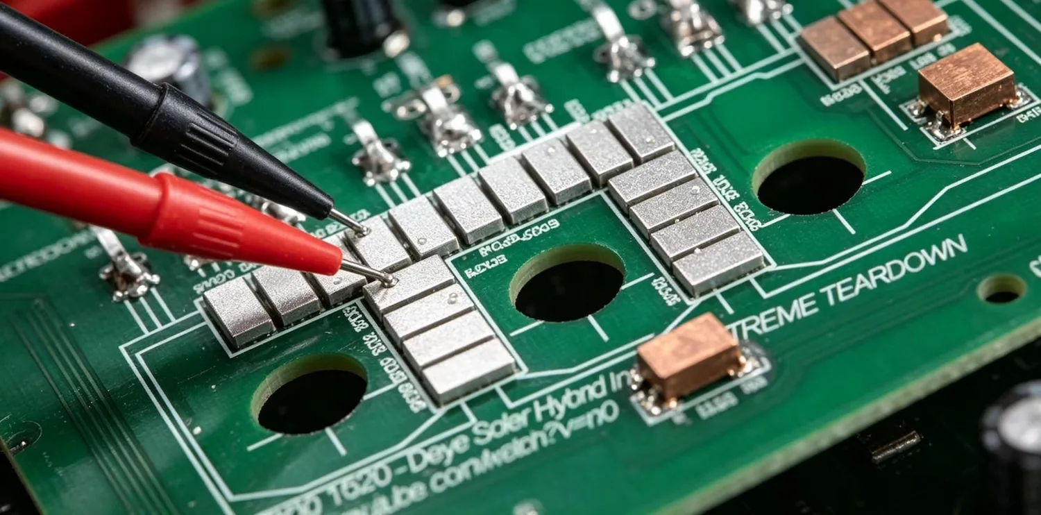
How to Increase PCB Current Capacity Without Widening Copper Traces?
How to Increase PCB Current Capacity Without Widening Copper Traces?
You calculate the required PCB trace width, only to discover that the board simply doesn’t have enough space.
What can you do when a PCB needs to carry more current but widening the copper traces is not an option?
For high-current power circuits, there are several ways to improve current-carrying capability without changing the overall PCB layout. Some involve optimizing the existing copper, while others add new conductive paths.
Improving PCB current capacity is not always about making copper traces wider. Depending on the PCB design, engineers can increase the available conductive area by using thicker copper, adding solder reinforcement, connecting multiple copper layers with via arrays, or installing additional copper busbars.
Here are four practical approaches worth considering.
1. Check the Allowable Temperature Rise First
Before changing the PCB design, check whether the trace width calculation uses a realistic temperature-rise limit.
Many online PCB trace calculators use a default temperature rise of 10°C. Depending on the application, a higher temperature rise may be acceptable.
For example, some industrial power circuits can be designed around a 20°C temperature rise, provided the PCB, components and surrounding materials remain within their specified temperature limits.
However, this does not mean that every circuit can safely operate at a higher temperature. Continuous current, ambient temperature, airflow, nearby components and operating conditions all matter.
The key is to establish the actual thermal limits before increasing the allowable temperature rise.
For trace sizing, use the applicable IPC-2152 design guidance or validated simulation and testing rather than relying on a single fixed width for a given current.
2. Use Thicker Copper
One straightforward way to reduce PCB trace resistance is to increase the copper thickness.
A common PCB copper thickness is:
| Copper Weight | Approximate Thickness |
|---|---|
| 1 oz | 35 μm |
| 2 oz | 70 μm |
| 3 oz | 105 μm |
| 5 oz | 175 μm |
For example, changing from 1 oz to 2 oz copper approximately doubles the copper cross-sectional area for the same trace width.
This can reduce resistance and help improve current-carrying capability without widening the trace.
However, thicker copper may increase PCB cost and affect minimum trace spacing, etching accuracy and manufacturing capability. Very heavy copper also requires checking with the PCB manufacturer before finalizing the design.
3. Use Solder Reinforcement on Exposed Copper Traces
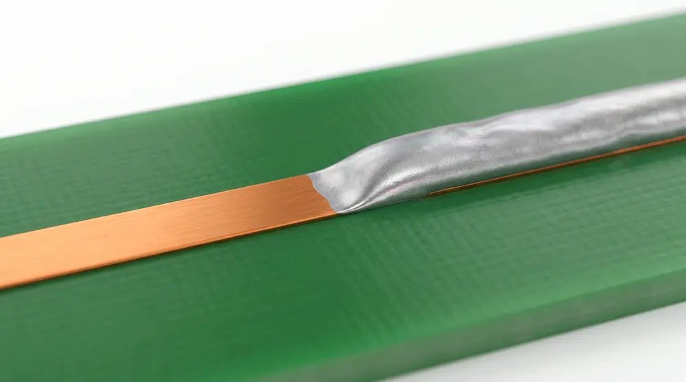
Another approach is to leave selected copper traces exposed and apply additional solder over them.
This is commonly called solder reinforcement or solder coating.
The additional solder increases the conductive cross-section and can reduce the overall resistance of the reinforced section.
However, solder is significantly less conductive than copper. It should not be treated as an equivalent replacement for copper foil.
The actual improvement depends on the solder alloy, solder thickness, coverage and connection quality.
This method may be useful for selected power traces, but solder thickness and coverage can vary during production. It is important to verify the result through resistance measurements and temperature-rise testing.
4. Use Via Arrays to Connect Multiple Copper Layers
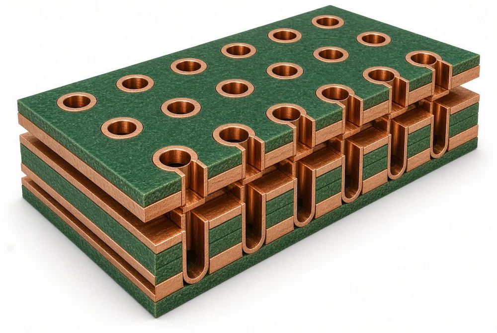
If the PCB has multiple copper layers, via arrays can help distribute current between them.
Instead of keeping the current on one surface layer, properly designed vias connect the top, bottom and internal copper layers, allowing them to share the current.
For example, a row or array of plated through-holes can connect parallel copper paths on different layers.
The design should consider:
- Number and diameter of vias
- Plated copper thickness inside each via
- Copper thickness and width of each connected layer
- Via spacing and current distribution
- Local heating around the vias
Simply adding more vias does not guarantee better current capacity. Their electrical resistance and thermal performance must be evaluated as part of the complete current path.
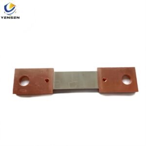
5. Add a Copper Busbar or SMD Copper Jumper
When PCB space is severely limited, adding a separate copper conductor may be a more practical solution.
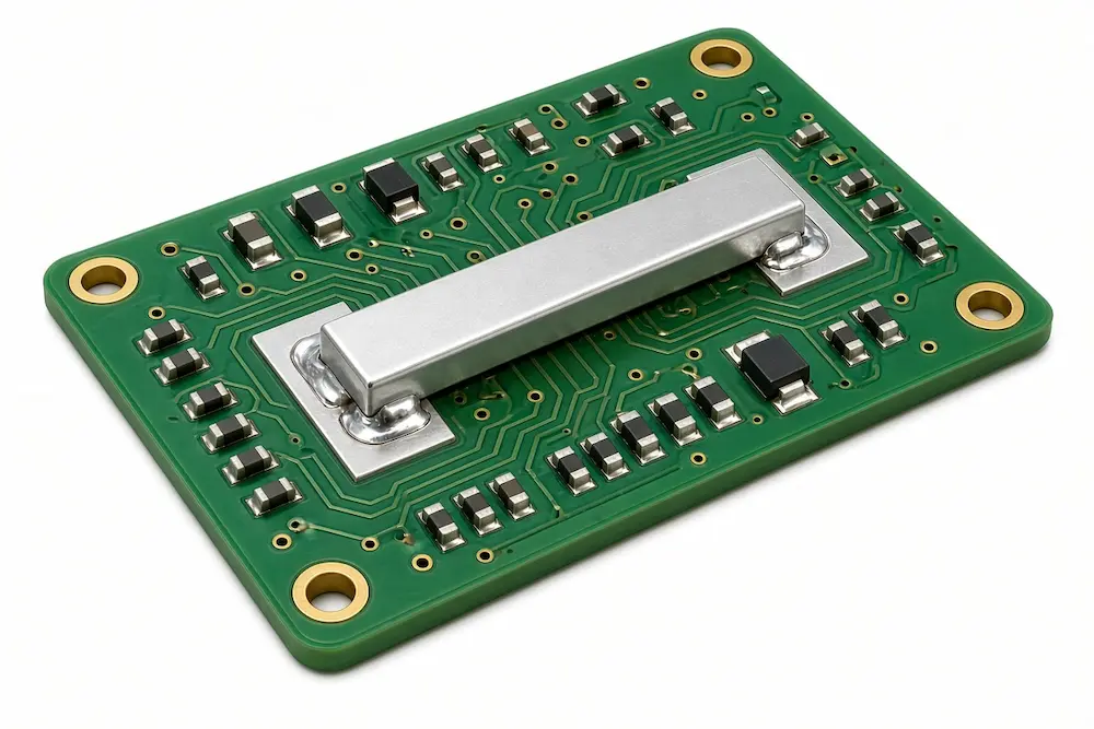
Instead of increasing the width or thickness of the PCB copper, a copper bar is mounted and soldered onto dedicated PCB pads.
This creates an additional conductive path above the PCB surface.
Depending on the design, the solution can use:
- Custom copper busbars
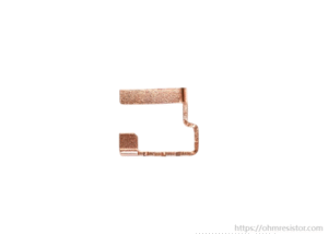
- SMD copper jumpers
- Metal strip conductors
- Other application-specific copper structures
Compared with reinforcing the PCB copper alone, an external copper conductor can provide a much larger conductive cross-section without requiring a wider PCB trace.
For example, multiple short copper jumpers can be arranged along a high-current PCB path. The design may also use segmented bars rather than one long copper bar, depending on mechanical and thermal requirements.
SMD Copper Jumpers for High-Current PCB Applications
SMD copper jumpers are worth considering when a compact, fixed-shape metal conductor is needed.
They can be designed with different lengths, widths and thicknesses to match PCB pad layouts and current-path requirements.
Compared with manually soldered copper braid, SMD copper jumpers offer defined dimensions and can be placed using SMT equipment.
One important process limitation: the SMD copper jumper discussed here is designed for reflow soldering only. It is not suitable for direct wave soldering.
Before selecting this solution, check the PCB pad design, soldering process, jumper dimensions and available assembly space.
How to Choose the Right Method?
Each method addresses a different design limitation.
| Method | Main Advantage | Main Consideration |
|---|---|---|
| Higher allowable temperature rise | May reduce required trace width | Must stay within thermal limits |
| Thicker copper | Reduces trace resistance | Higher PCB manufacturing cost |
| Solder reinforcement | Adds conductive material to exposed traces | Solder has lower conductivity than copper |
| Via arrays | Connects multiple PCB copper layers | Requires careful via and layer design |
| Copper busbar or SMD jumper | Adds a separate, larger conductive path | Requires space, pads and reliable solder joints |
The best solution depends on the required current, PCB construction, thermal limits, production process and available space.
Conclusion
When a PCB trace cannot be widened, increasing current capacity does not have to mean redesigning the entire board.
Depending on the application, designers can consider thicker copper, solder reinforcement, via arrays or an additional copper conductor.
For applications where PCB space is limited but a larger conductive cross-section is needed, a copper busbar or SMD copper jumper may be a practical option.
The final design should always be checked through electrical resistance measurements and temperature-rise testing under actual operating conditions.
Looking for a compact copper conductor for your high-current PCB design?
Explore our SMD Zero Ohm Jumper for available configurations and customization options.
Contact us with your required dimensions and PCB layout to discuss a suitable solution.
Apply this to your component selection
For a specific project, share your part number or drawing, quantity, and key operating conditions. We can help review your requirements and coordinate with our manufacturing resources.