Why Does an SMD Copper Jumper Shift During Reflow Soldering?
Why Does an SMD Copper Jumper Shift During Reflow Soldering?
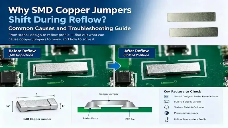
SMD copper jumper shift during reflow soldering can occur when solder paste deposition, PCB pad design, surface conditions, component placement, or the reflow profile is not properly controlled. Understanding these factors can help engineers identify the cause and improve soldering consistency.
A small SMD copper jumper may appear correctly positioned during pre-reflow inspection, yet become misaligned after passing through the reflow oven.
This issue can be frustrating for PCB assembly engineers, especially when the component appears correctly placed before soldering.
In SMT assembly, component movement during reflow is not necessarily caused by the pick-and-place machine. Uneven solder wetting, excessive or unbalanced solder paste deposits, pad geometry, surface condition, and reflow settings can all contribute to the problem.
Based on our experience supporting SMD metal jumper applications, the following checks can help narrow down the possible causes.
1. Common Causes of SMD Copper Jumper Shift During Reflow
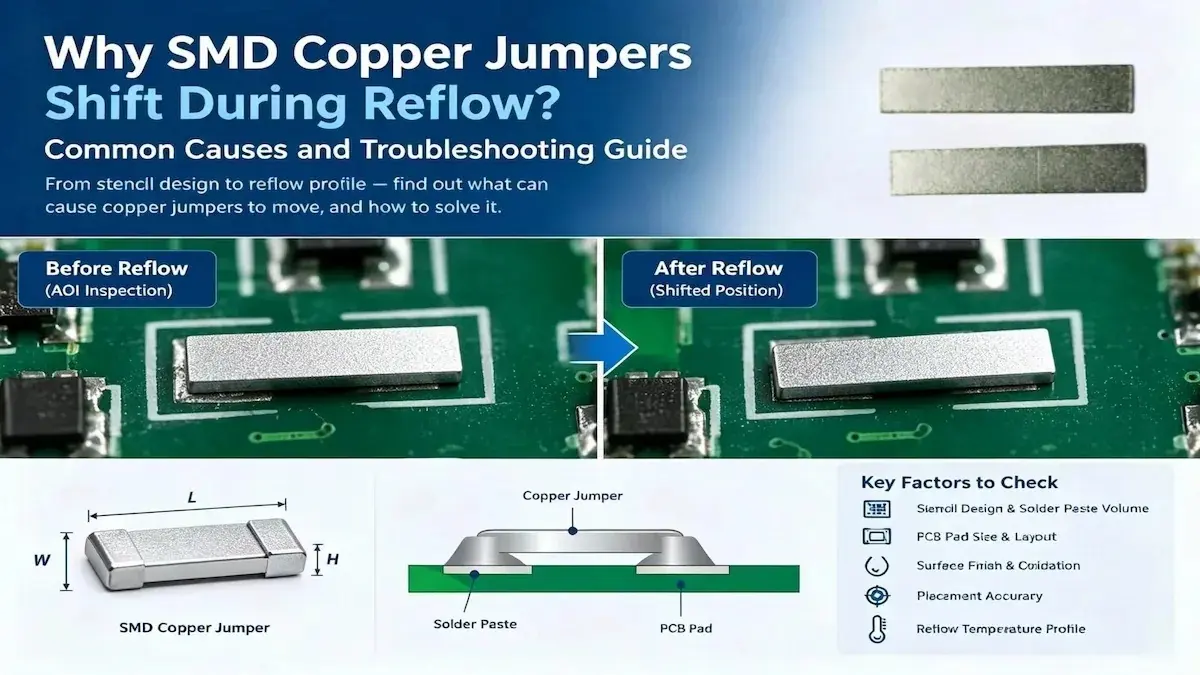
Several factors can contribute to component movement after solder paste melts. In many cases, the issue results from a combination of solder paste distribution, PCB footprint design, surface conditions, placement accuracy, and thermal behavior.
Before changing the assembly process, compare the component position before and after reflow and inspect the solder joints. This helps establish whether the movement is repeatable and which process variables require further investigation.
2. Check the Stencil Aperture Design and Solder Paste Volume
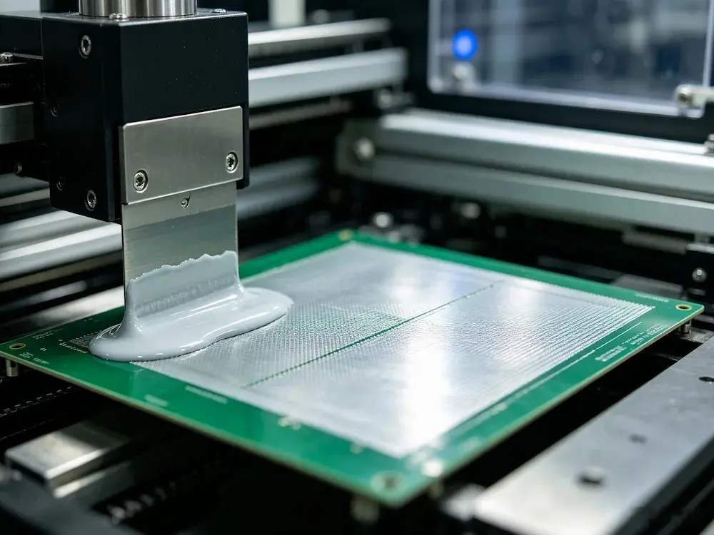
Solder paste deposition is one of the first areas to investigate when a copper jumper shifts during reflow.
If the stencil aperture is too large, excessive solder paste may be deposited beneath the component. As the solder melts, the component may move if the solder deposits or wetting forces are unbalanced.
On the other hand, an aperture that is too small may result in insufficient solder paste, increasing the risk of weak or incomplete solder joints.
What to check:
- Compare the stencil aperture dimensions with the PCB pad dimensions.
- Check the actual solder paste deposits before placement, preferably using solder paste inspection (SPI).
- Compare the paste deposits on both sides of the jumper.
- Review stencil thickness and aperture geometry if excessive or inconsistent paste deposition is observed.
The objective is not simply to minimize solder paste volume. The deposits must provide sufficient solder for reliable joints while maintaining balanced wetting conditions during reflow.
3. Check the PCB Pad Dimensions
The relationship between the copper jumper dimensions and the PCB pads can affect component alignment during soldering.
If the pads are excessively large relative to a small, lightweight jumper, the component may be more susceptible to movement when the solder melts. If the pads are too small, there may be insufficient soldering area for reliable joint formation.
However, pad size alone does not determine the outcome. Pad geometry, solder paste distribution, component placement, and local thermal conditions must also be considered.
What to check:
- Compare the component footprint with the actual jumper dimensions.
- Confirm that the pads provide adequate soldering area and mechanical support.
- Check whether the solder paste deposits are symmetrical.
- Review the recommended PCB footprint for the specific jumper design.
For customized SMD copper jumpers, reviewing the component dimensions and proposed PCB pad layout together can help identify potential assembly issues before larger production quantities are released.
4. Check the Copper Surface Condition and Plating
Surface condition can influence solder paste wetting and the balance of forces acting on a component during reflow.
Oxidation or an unsuitable surface finish may reduce solderability or cause uneven wetting. When solder does not wet the component terminals and PCB pads consistently, the expected self-alignment effect may be reduced.
What to check:
- Inspect the copper jumper for oxidation, contamination, or visible surface defects.
- Confirm that the specified plating or surface treatment is suitable for the intended soldering process.
- Verify compatibility between the component finish, PCB surface finish, and solder paste.
- Review storage and handling conditions if surface deterioration is suspected.
For SMD copper jumpers, appropriate surface protection and controlled plating are important considerations. The actual finish should be selected according to the application and assembly requirements.
5. Check the Pick-and-Place Position
A jumper that appears correctly positioned before reflow may still have a small placement offset that becomes more noticeable after soldering.
During reflow, molten solder develops surface-tension forces that can help pull a component toward alignment. This self-alignment effect is not guaranteed to correct every placement error. Uneven wetting or asymmetric solder deposits can instead cause the component to move away from its intended position.
What to check:
- Compare the pre-reflow and post-reflow component positions.
- Review the placement coordinates and rotation settings.
- Check the nozzle, component pickup, and placement-height settings if the problem is repeatable.
- Compare results from automatic placement with any manually placed samples, where practical.
If the component is consistently shifted in the same direction, investigate the placement position and solder paste distribution together rather than assuming that the placement machine is the only cause.
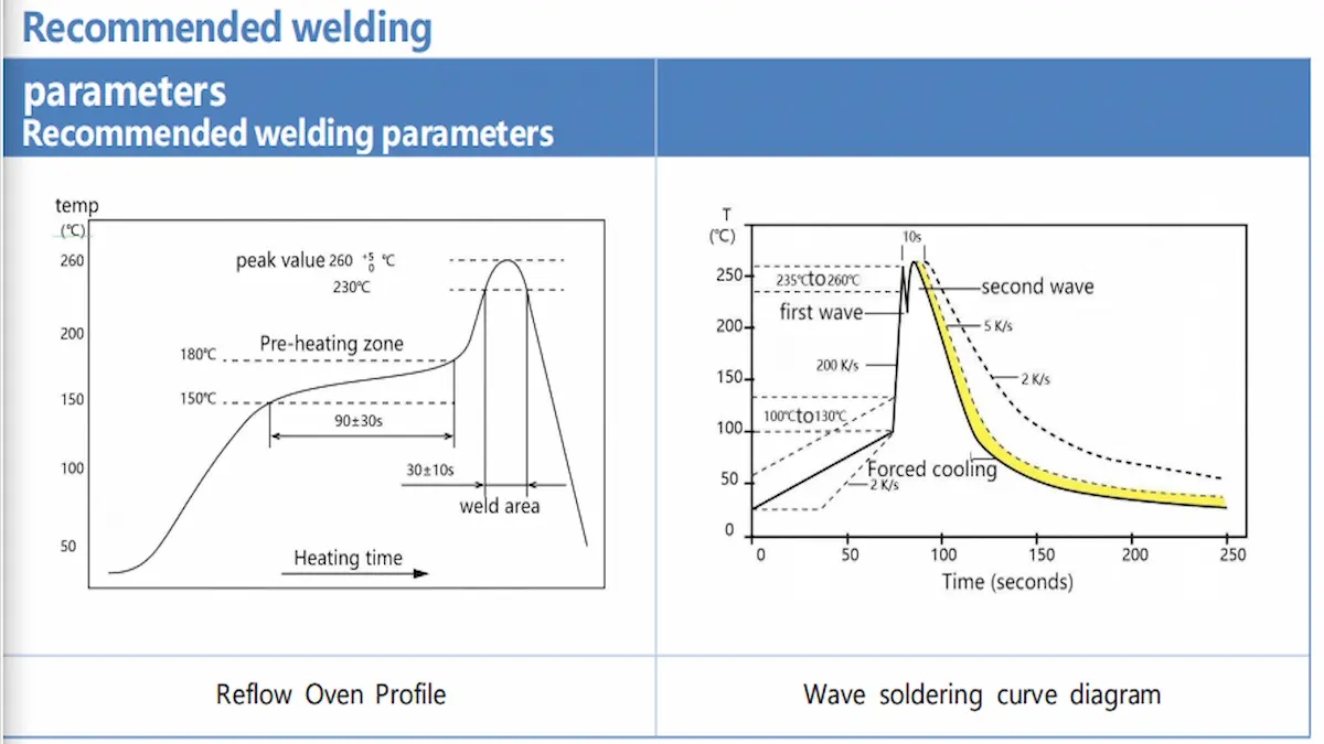
6. Review the Reflow Temperature Profile
The reflow profile can also influence component movement and solder joint formation.
Copper has relatively high thermal conductivity, and the thermal mass of the component and surrounding PCB copper can affect local heating behavior. If the two sides of the component heat or wet differently, the resulting forces may become unbalanced.
An unsuitable heating ramp, insufficient time at the appropriate temperature, or process conditions outside the recommended window may also contribute to assembly problems. Airflow or conveyor-related effects should be investigated when there is evidence that they are affecting component stability.
What to check:
- Measure the actual temperature profile on a representative PCB assembly.
- Confirm that the solder paste manufacturer’s recommended process window is followed.
- Check whether the two sides of the jumper experience substantially different thermal conditions.
- Review airflow, conveyor movement, and possible mechanical interference if the component is displaced despite apparently balanced solder joints.
Do not increase the oven temperature or change the heating rate solely because a jumper has shifted. First determine whether the problem is related to insufficient heating, uneven wetting, excessive paste, or another process factor.
7. How to Reduce the Risk of SMD Copper Jumper Shift During Reflow
For customized SMD metal jumpers, early coordination between the component supplier, PCB designer, and assembly engineer can help reduce avoidable process issues.
Before sample evaluation, it is useful to confirm:
- Component dimensions and mounting height
- PCB pad layout and stencil aperture design
- Copper material and surface finish
- Solder paste and reflow process requirements
- Inspection criteria for component alignment and solder joint quality
No single adjustment guarantees a solution in every case. The appropriate corrective action should be based on inspection results and, where necessary, controlled process trials.
8. A Practical Troubleshooting Checklist for SMD Copper Jumpers
When an SMD copper jumper passes pre-reflow inspection but shifts after soldering, review the following items in sequence:
- Solder paste: Are the deposits excessive, insufficient, or uneven?
- PCB footprint: Are the pad dimensions and geometry appropriate for the jumper?
- Surface condition: Is the component finish clean and suitable for soldering?
- Placement: Is the jumper centered and seated consistently in the paste?
- Reflow process: Are the temperature profile, heating balance, and conveyor conditions appropriate?
Where possible, compare the same component across multiple boards and record the direction and amount of movement. A repeatable pattern can help distinguish a component-specific issue from a broader assembly-process problem.
Need Help Evaluating an SMD Copper Jumper?
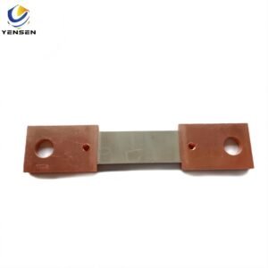
OHM Resistor supports customers with SMD metal jumpers, copper jumper bars, and customized dimensions through our manufacturing partners in China.
If you are evaluating a new jumper design or investigating component movement during reflow, you can share the component drawing, PCB footprint, soldering conditions, and relevant inspection photos for an initial review.
Contact OHM Resistor to discuss your SMD jumper requirements and product options.
[Browse SMD Jumper Products](https://ohmresistor.com/product/smd-zero-ohm-jumper
Apply this to your component selection
For a specific project, share your part number or drawing, quantity, and key operating conditions. We can help review your requirements and coordinate with our manufacturing resources.